Etched copper: Adapting PCB techniques
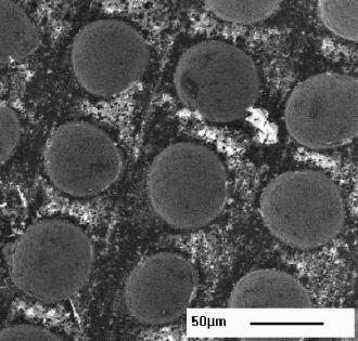
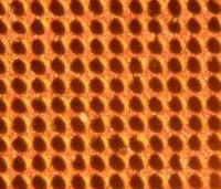
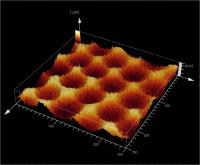
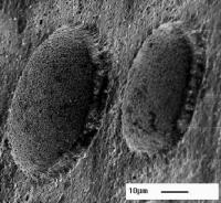
A simple method for making printed circuit boards for electronic applications is to take a copper clad board and coat it with an ultraviolet-sensitive photoresist. The pattern of conducting tracks are imaged onto the board with an ultraviolet light and developed to leave the photoresist where the copper is required. When the board is placed in acid, the exposed copper is etched away forming the track pattern. The same process can be used to etch craters into a copper clad board. If the craters are etched until they join up they create a landscape of sharp pinnacles which when hydrophobized provide a superhydrophobic surface. Read more about the process in the publication below.
Publication
![]()
N.J. Shirtcliffe, G. McHale, M.I. Newton, G. Chabrol and C.C. Perry,
Wetting and wetting transitions on copper-based super-hydrophobic surfaces,
Langmuir 21 (3) (2005) 937-943.
Via ACS server
Wetting and wetting transitions on copper-based super-hydrophobic surfaces,
Langmuir 21 (3) (2005) 937-943.
Via ACS server